PMOS vs NMOS: Key Differences & How to Choose the Right MOSFET
If you're picking a MOSFET for a switching circuit, the first question isn't "which part number" - it's N-channel or P-channel? Get this wrong and you'll fight gate drive problems, burn power in places you shouldn't, or pay more for silicon you don't need.
Here's the short answer: NMOS wins on efficiency and cost. PMOS wins on gate-drive simplicity. If you're switching loads above 10A, the decision makes itself - NMOS, full stop. Below 2A, especially for high-side switching from a battery, PMOS saves you a charge pump and a handful of passives. From our Shenzhen distribution data (2025–2026), NMOS parts outsell PMOS roughly 8:1 by volume - but in battery-powered designs under 2A, PMOS holds a steady niche that isn't going anywhere.
The trick is knowing where the tradeoffs actually matter. This guide covers the physics, the dollars, and the real-world gotchas.
PMOS vs NMOS: Quick Comparison Table
| Parameter | NMOS (N-Channel) | PMOS (P-Channel) |
|---|---|---|
| Charge Carrier | Electrons (high mobility, ~1,400 cm²/V·s) | Holes (low mobility, ~450 cm²/V·s) |
| Gate Voltage to Turn ON | Positive Vgs (gate > source by Vth) | Negative Vgs (gate < source by |Vth|) |
| Typical Vgs(th) | 1–4V (logic-level: 1–2V) | −1 to −4V (logic-level: −1 to −2V) |
| RDS(on) for Same Die Area | Low (reference) | ~2–3× higher |
| Relative Die Size (same RDS(on)) | 1× | ~2–3× larger |
| Switching Speed | Fast | ~2–3× slower (higher gate charge for same RDS(on)) |
| Cost (same RDS(on) rating) | Lower | Higher (larger silicon area) |
| Low-Side Switch | Ideal - source to ground, gate drive trivial | Inconvenient - source to load, gate drive referenced to floating node |
| High-Side Switch | Needs bootstrap/charge pump to generate gate voltage above rail | Ideal - pull gate low (to ground) to turn on |
| Common Applications | DC-DC converters, motor drives, SMPS, CPU power, low-side load switches | High-side load switches, reverse polarity protection, battery disconnect, inrush limiting |
| Typical Voltage Range | 20V–650V+ widely available | Most practical below 200V (becomes expensive/uncommon above) |
| Body Diode Direction | Source → Drain (cathode at drain) | Drain → Source (cathode at source) |
Why NMOS Is More Efficient - The Physics Behind the Difference
The performance gap between NMOS and PMOS isn't a manufacturing artifact. It's physics.
In silicon, electrons move roughly 3 times faster than holes under the same electric field. NMOS uses electrons as its majority carrier. PMOS uses holes. This means:
- For the same die area: an NMOS transistor achieves ~3× lower RDS(on) than a PMOS. Or, flipped around: to match an NMOS's RDS(on), a PMOS needs ~2–3× the silicon area - which means a larger package, higher cost, and higher gate capacitance.
- Gate charge penalty compounds it: because the PMOS die is larger to achieve the same RDS(on), its gate capacitance (and therefore Qg) is also larger. Switching losses (P = Qg × Vgs × f) scale with Qg - so the PMOS loses on both conduction and switching.
- At high currents, the gap widens: the RDS(on) gap between NMOS and PMOS of similar cost grows with current rating. At 1A, a PMOS might be 1.5× the cost of an equivalent NMOS. At 20A, it can be 3–5× - and the available PMOS selection shrinks dramatically.
This is why every high-efficiency power converter - your phone charger, your server PSU, the VRM on your motherboard - uses NMOS almost exclusively. When efficiency targets push past 90%, PMOS conduction losses become impossible to justify.
When to Choose NMOS
High-current switching (>10A)
Above 10A, the economics force NMOS. The PMOS parts that can handle 20A+ with reasonable RDS(on) are expensive, large (TO-220/TO-247), and have limited second-source options. NMOS at these currents is a commodity - multiple manufacturers, competitive pricing, and packages from SOT-23 to TO-247.
Low-side switching
When the MOSFET sits between the load and ground, NMOS is the natural choice. The source terminal connects directly to ground, so driving the gate is trivial: a 3.3V or 5V logic signal (plus a gate resistor) is all you need. This is the standard configuration for relay drivers, solenoid controllers, LED strips, and virtually every low-side switch in existence.
DC-DC converters and SMPS
Buck converters, boost converters, flyback supplies - the switching MOSFET in these topologies is almost always NMOS. The combination of low RDS(on), low Qg, and fast switching is non-negotiable when you're trying to hit 85%+ efficiency at 500 kHz. Per the TI datasheets for their TPS54xx and LM2xxx families, the reference designs exclusively use N-channel MOSFETs for both the high-side and low-side positions - with a bootstrap circuit handling the high-side gate drive.
When every milliohm counts
If your design's thermal budget is tight and you need the lowest possible RDS(on) in the smallest package, NMOS is the only answer. A 30V NMOS in SOT-23 can achieve <30 mΩ RDS(on). A 30V PMOS in the same package will be closer to 60–90 mΩ - more than double the heat for the same current.
When to Choose PMOS
High-side switching without extra circuitry
This is PMOS's killer feature. To switch a load on the high side (between the positive rail and the load), you need the MOSFET between VCC and the load. With an NMOS, the source voltage rises to nearly VCC when the FET is on - which means the gate must be driven above VCC by at least Vth to keep the FET enhanced. That requires a bootstrap capacitor, a charge pump, or a dedicated gate driver IC.
With a PMOS? Pull the gate LOW to turn it on. Pull it HIGH (to VCC) to turn it off. One resistor, one GPIO pin from your MCU. Done. This simplicity is why PMOS dominates low-current power path switching in battery-powered products.
Battery-powered devices (<2A load)
In a product that runs from a single LiPo cell (3.7–4.2V), a PMOS high-side switch lets you disconnect the load with a single MCU pin. No charge pump, no bootstrap capacitor that needs periodic refreshing, no minimum switching frequency. Just a logic-level PMOS and a pull-up resistor. The slightly higher RDS(on) is negligible at sub-2A currents - we're talking tens of milliwatts of extra loss in exchange for a dramatically simpler BOM.
Reverse polarity protection
A PMOS with its gate to ground and source to the input rail forms a near-ideal reverse polarity protector: when the input is connected correctly, the body diode conducts briefly, the gate-source voltage becomes negative, and the FET turns on fully - presenting only its RDS(on) to the load. If the input is reversed, Vgs is zero (or positive) and the FET stays off. Compare this to a series Schottky diode: at 2A, a diode drops ~0.4V and dissipates 0.8W. A PMOS with 30 mΩ RDS(on) drops 60 mV and dissipates 120 mW - a 6× reduction in power loss.
Inrush current limiting and battery disconnect
BMS designs often use PMOS for charge/discharge FETs because the gate drive is referenced to the battery positive terminal - no floating gate drive needed. Similarly, hot-swap controllers frequently use PMOS for the main pass element when the input voltage is below ~20V and the current is moderate.
What About Cost and Availability?
From our Shenzhen distribution data (2025–2026), here's what the market looks like for common SOT-23 MOSFETs:
| Category | NMOS (e.g., AO3400A, SI2302DS) | PMOS (e.g., AO3401A, SI2301DS) |
|---|---|---|
| Volume Price (3k+ reel) | $0.02–0.05/unit | $0.04–0.08/unit |
| Sample/Low Volume | $0.05–0.10/unit | $0.08–0.15/unit |
| Availability (SOT-23) | Broad - 20+ manufacturers | Moderate - 8–12 active sources |
| Second-Source Options | Excellent - virtually every fab has a line | Good below 30V; limited above 100V |
| Lead Time (typical, 2025–2026) | 2–6 weeks | 4–10 weeks for less common specs |
The price gap narrows at very low currents. For a 100 mA load switch, the difference between a $0.03 NMOS and a $0.05 PMOS is negligible - and the PMOS saves you a gate driver. For a 20A motor drive, the NMOS at $0.25 vs a PMOS at $0.80 (if you can find one) is a no-brainer.
Contact ICMASS for current pricing on your specific requirements. We stock a full range of NMOS and PMOS parts in SOT-23, TO-220, and SO-8 packages from AOS, Infineon, Vishay, and onsemi.
Common Mistakes When Choosing Between PMOS and NMOS
Mistake 1: Using a PMOS at 12V with a 3.3V GPIO - without checking Vgs(max)
A logic-level PMOS turns on when the gate is pulled LOW relative to the source. If your source is at 12V and your MCU GPIO pulls the gate to 0V, Vgs = −12V. Many PMOS parts have a Vgs(max) of ±8V or ±12V - you're right at or over the limit. One transient and the gate oxide punches through. Fix: use a level-shift circuit (NPN transistor + two resistors) or pick a PMOS rated for ±20V Vgs.
Mistake 2: Forgetting the body diode direction
NMOS body diode: anode at source, cathode at drain. PMOS body diode: anode at drain, cathode at source. This is the opposite direction. If you swap an NMOS for a PMOS (or vice versa) without checking, the body diode will conduct when you don't expect it - or block current flow entirely. Always draw the body diode on your schematic. Always.
Mistake 3: Assuming PMOS gate drive is always "just one resistor"
It is - if the supply voltage is within the gate rating of the PMOS and your MCU can tolerate the supply voltage on its GPIO (with a pull-up). But at higher voltages, you need a level translator. At very low voltages (<3V), a standard PMOS with Vgs(th) of −2V might not turn on fully with a 3.3V rail - you need a logic-level part with Vgs(th) around −1V. The "just one resistor" claim comes with an asterisk.
Mistake 4: Using NMOS for high-side switching without a bootstrap when PWM is involved
An NMOS high-side switch driven by a bootstrap circuit works - but only if you're switching regularly. The bootstrap capacitor needs to be refreshed periodically (every few milliseconds, depending on the capacitor value and leakage). If you try to hold the high-side NMOS ON continuously (100% duty cycle), the bootstrap capacitor discharges through leakage and the gate voltage collapses. The FET enters its linear region, RDS(on) skyrockets, and it burns. For static ON/OFF high-side switching at moderate currents, PMOS is the simpler and safer choice.
Mistake 5: Picking a PMOS by RDS(on) alone, ignoring gate charge
Because PMOS dies are larger for a given RDS(on), their total gate charge (Qg) is proportionally higher. In a PWM application at 50 kHz, a PMOS with nice RDS(on) specs might have 3× the gate charge of an NMOS with similar RDS(on). The switching losses dominate and the PMOS runs hotter - despite the "good" RDS(on) number on the datasheet front page. Check Qg and calculate switching loss before committing.
Frequently Asked Questions About PMOS vs NMOS
Q1: Can I replace an NMOS with a PMOS in the same circuit?
A: Not directly. Aside from the opposite gate drive polarity (NMOS needs positive Vgs, PMOS needs negative Vgs), the body diode points the other direction - which changes how current flows when the FET is off. You also need to flip the source and drain connections: in an NMOS low-side switch, source goes to ground; in a PMOS high-side switch, source goes to the positive rail. A direct footprint swap without schematic changes will not work.
Q2: Why is PMOS more expensive than NMOS?
A: Two reasons. First, physics: holes move slower than electrons in silicon, so a PMOS needs ~2–3× more die area to achieve the same RDS(on) as an NMOS. More silicon = higher cost. Second, volume: NMOS is used in virtually every power converter, CPU VRM, and motor drive on the planet. The manufacturing volume is orders of magnitude higher, which drives down per-unit cost. PMOS is a smaller market, so it doesn't benefit from the same economies of scale.
Q3: When should I use an NMOS for high-side switching instead of a PMOS?
A: When (a) the load current is above ~5A - the higher cost and RDS(on) of a PMOS become hard to justify, (b) you're doing PWM at high frequency, where NMOS switching speed matters, or (c) the input voltage exceeds ~20V, where PMOS options become scarce. In these cases, use an NMOS with a bootstrap gate driver (for switching applications) or a charge pump (for static ON applications). The extra BOM cost of the gate driver is offset by the cheaper, more efficient NMOS.
Q4: Can I drive a PMOS directly from a 3.3V MCU pin?
A: Yes, with three conditions: (1) the supply rail you're switching is 3.3V (so Vgs = −3.3V when the GPIO pulls low - enough to enhance a logic-level PMOS with Vgs(th) < −1.5V), (2) the supply rail voltage doesn't exceed the MCU GPIO's maximum voltage rating when pulled high through the pull-up resistor, and (3) you're using a logic-level PMOS rated for low Vgs(th). If the supply rail is 5V or higher, you need a level translator between the MCU and the PMOS gate - otherwise the GPIO might not pull high enough to turn the PMOS fully off, or the supply voltage may damage the GPIO.
Q5: What's the practical current limit for PMOS in a high-side switch?
A: For SOT-23 packages, ~2–3A continuous with good PCB copper. For SO-8, ~5–8A. For TO-220/TO-252, 10–20A. Beyond 20A, PMOS selection becomes extremely limited - you'll spend more time searching for a part that exists than designing the circuit. At 30A+, use NMOS with a gate driver. The semiconductor industry simply doesn't invest in large-die PMOS development because the market is too small.
Q6: Is a PMOS reverse polarity protector better than a Schottky diode?
A: For power loss, yes - dramatically. At 2A, a Schottky diode drops ~0.4V (0.8W loss). A PMOS with 30 mΩ RDS(on) drops 60 mV (120 mW loss) - roughly 7× less power. The diode costs $0.05 and uses one component. The PMOS solution costs ~$0.10–0.20 and uses 3 components (PMOS + gate resistor + zener for gate protection if needed). For currents above 500 mA where power dissipation matters, the PMOS wins. For a 100 mA signal line, the diode is simpler and good enough.
Related information




-
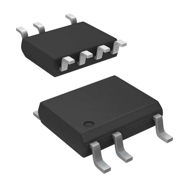
LNK304DN-TL Power Integrations
-
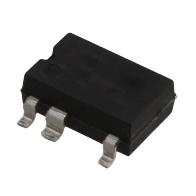
LNK304GN-TL Power Integrations
-
LNK304DG-TL Power Integrations
-
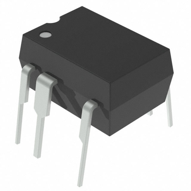
TNY277PN Power Integrations
-
TNY276PN Power Integrations
-
TNY278PN Power Integrations
-
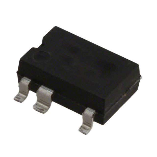
TNY278GN-TL Power Integrations
-
TNY280GN-TL Power Integrations
-
TOP266KG-TL Power Integrations
-
TOP258PN Power Integrations
-
TOP253PN Power Integrations
-
TOP253PNAU Power Integrations

- 1500+ Daily average RFQ Volume

- 20,000.000 Standard Product Unit

- 1800+ Worldwide Manufacturers

- 15,000+ In-stock Warehouse