LM317 Pinout, Specifications & Common Mistakes
LM317 Pinout, Specifications & Common Mistakes | ICMASS
The LM317 is the most widely used adjustable linear voltage regulator ever made. Three pins, two external resistors, and you get any output from 1.25V to 37V at up to 1.5A. Simple enough to use in your sleep. But the pinout is NOT what your schematic symbol shows, the tab is live at the output voltage, and a potentiometer wiper going open can send full unregulated voltage to your load. Here's the full reference, including the mistakes we see engineers make over and over — sourced from the forums where they come to debug them.
LM317 Pinout and Pin Functions
Critical: schematic symbols lie. Many CAD libraries draw the LM317 with pins in the order INPUT-ADJUST-OUTPUT left to right. The physical TO-220 package is ADJUST-OUTPUT-INPUT (left to right, labeled face toward you). EasyEDA shipped libraries with this error. TI themselves published a SOT-223 drawing in PCN# 20250618000.1 that appeared to swap ADJ and VIN — later confirmed as a documentation bug. Always wire by pin number, not by symbol order.
R1 = 120Ω or 240Ω? The datasheet says 240Ω (5.2mA minimum load). Forum consensus from EEVblog and StackExchange: 120Ω is safer. The LM317 needs 3.5–10mA minimum load current to regulate. 240Ω meets the typical spec (5.2mA) but not the worst-case (10mA). At 120Ω you get 10.4mA — guaranteed regulation even with zero external load and a worst-case part. For bench supplies, 240Ω is fine. For production, use 120Ω.
D1 and D2 are not optional when Cout > 10µF or Cadj > 5µF. D1 (1N4002, cathode to VIN) protects against input short: Cout discharges through D1 instead of backwards through the LM317. D2 (cathode to VOUT) protects against output short: Cadj discharges through D2 instead of the ADJ pin. Cost: two 1N4002s. Cost of not having them when you need them: a dead regulator and an afternoon of debugging.
Cin is not optional if the input lead is > 6 inches. Input wiring inductance + Cin forms an LC tank that can ring to 2× the supply voltage at power-on, exceeding the 40V input-output differential limit. A 0.1µF ceramic at the input pin + an electrolytic (10µF–100µF) at the board input kills the ringing.
LM317 Key Specifications
| Parameter | Value |
|---|---|
| Output Voltage Range | 1.25V to 37V |
| Input-Output Differential | 3V to 40V (dropout ~2–3V) |
| Output Current | 1.5A max (thermally limited) |
| Reference Voltage | 1.25V typical (between VOUT and ADJ) |
| Minimum Load Current | 3.5mA typ, 10mA max |
| Line Regulation | 0.01%/V typ |
| Load Regulation | 0.1% typ |
| Ripple Rejection | 65dB typ @ 120Hz (improves with CADJ) |
| ADJ Pin Current (IADJ) | 50µA typ, 100µA max |
| Thermal Shutdown | ~165°C junction |
| Packages | TO-220, SOT-223, TO-252, TO-3 |
Common Mistakes When Using the LM317
1. Counterfeit parts — the #1 LM317 problem on forums. Cheap LM317s from eBay, Amazon, or AliExpress are frequently re-labeled LM317L parts rated for only ~100mA. Symptoms: regulates fine at light load, output collapses above 100–200mA. If your "LM317T" can't deliver 500mA without sagging, it's probably an LM317L with a new label. Buy from authorized distribution or a supplier that verifies lots — ICMASS tests incoming LM317 batches for full 1.5A current capability.
2. Potentiometer wiper failure destroys the load. If you use a pot as R2 to set VOUT and the wiper goes open (dirty contact, vibration, oxidation), the ADJ pin floats and VOUT jumps to nearly VIN — potentially destroying everything downstream. Fixes: wire the pot as the upper leg (R2 between OUT and ADJ) with a fixed resistor as the lower leg (R1 from ADJ to GND), so an open wiper sends ADJ to GND through R1 → VOUT = 1.25V minimum, not maximum. Or add a zener diode from ADJ to GND (e.g., 7.8V for a 9V output) to clamp the maximum. Always design the feedback network so the default failure mode is minimum voltage, not maximum.
3. The tab is live at VOUT, not GND. In the TO-220 package, the metal tab is internally connected to Pin 2 (VOUT). Bolting two LM317s to the same heatsink without insulation shorts their outputs together. Bolting a single LM317 to a grounded heatsink without a mica washer shorts the output to ground. Even with SOT-223, the exposed thermal pad is VOUT — don't connect it to a ground plane. Always use insulating mounting hardware if the heatsink touches anything conductive.
4. Omitting protection diodes with large output capacitors. If COUT > 10µF and the input gets shorted to ground, the charged output capacitor discharges backwards through the LM317's internal junctions. This can destroy the regulator. D1 (1N4002, cathode to VIN) provides a safe discharge path. Same logic for CADJ > 5µF: add D2 (cathode to VOUT). These two diodes cost pennies. The debug session they prevent costs hours.
5. Forgetting dropout voltage. The LM317 needs 2–3V headroom. 5V from a 6V supply won't work — the output sags and ripple rejection collapses. If VIN − VOUT < 3V, use an LDO like the AMS1117 (1.1V dropout). Also: at 1.5A with 10V drop, the LM317 dissipates 15W. The TO-220 junction hits 150°C in seconds without a heatsink. PD = (VIN − VOUT) × IOUT. Calculate it before you solder.
6. Trusting the schematic symbol instead of the datasheet pinout. Many EDA libraries draw the LM317 pins in INPUT-ADJUST-OUTPUT order. The physical package is ADJUST-OUTPUT-INPUT (Pin 1-2-3). EasyEDA shipped incorrect LM317 TO-220 symbols. TI themselves had a SOT-223 drawing error in a PCN document that appeared to swap pins. Don't trust the symbol — open the datasheet and verify Pin 1 = ADJ (left), Pin 2 = VOUT (center, also tab), Pin 3 = VIN (right).
7. Large Cout with no Cin — the power-up killer. At power-on with a large output capacitor and little or no input capacitance, the input-output differential can briefly see the full supply voltage while charging Cout through the regulator. Cable inductance can cause ringing to 2× supply voltage. The LM317's 40V maximum differential gets exceeded, and the part fails. Fix: always have more input capacitance than output capacitance at the regulator pins, or use a high-ESR electrolytic on the input to damp the LC resonance.
Where to Buy Genuine LM317
ICMASS stocks LM317T (TO-220), LM317MPX (SOT-223), and LM317L variants. Every lot is tested for full 1.5A output capability — no re-labeled LM317L parts. Contact us for current pricing. Volume pricing $0.04–$0.12/unit depending on package and quantity. Shenzhen stock, same-day dispatch before 15:00 CST.
Frequently Asked Questions
Q1: LM317T pinout — which pin is which?
A: Pin 1 = ADJ (left), Pin 2 = VOUT (center, also the metal tab), Pin 3 = VIN (right). Viewed from the front with the labeled side facing you and pins pointing down. Both TO-220 and SOT-223 use the same numbering. Many schematic symbols draw them in a different order — always wire by pin number, not symbol order. The tab is electrically VOUT, not GND. Insulate it from the heatsink unless your heatsink is floating.
Q2: Can I use LM317 to get output below 1.25V?
A: Not without an external negative supply. The internal reference is fixed at 1.25V between VOUT and ADJ. To get 0V output, you need to pull the ADJ pin to -1.25V using a negative charge pump or auxiliary winding. For most designs needing sub-1.25V, use a modern adjustable LDO with a lower reference (0.6V or 0.8V).
Q3: R1 = 240Ω or 120Ω?
A: 120Ω for production; 240Ω is fine for bench supplies. The 240Ω resistor gives 5.2mA minimum load — meets the 3.5mA typical spec, but not the 10mA worst-case. Using 120Ω (10.4mA) guarantees regulation even with zero external load and a worst-case part. On EEVblog, engineers who debugged "mysterious regulation failure at no load" consistently traced it to using R1 values above 120Ω on marginal parts. The extra 5mA of quiescent current is irrelevant in mains-powered designs; in battery-powered designs, consider the LM317L (100mA version, lower min load) instead.
Q4: How do I calculate the output voltage?
A: VOUT = 1.25 × (1 + R2/R1) + IADJ × R2. The IADJ term is typically 50µA × R2 — adds about 0.05V at R2=1kΩ. For most designs, the simplified formula VOUT = 1.25 × (1 + R2/R1) is within 2%. With R1 = 120Ω: for 5V, R2 = 360Ω; for 9V, R2 = 744Ω; for 12V, R2 = 1.03kΩ.
Q5: My eBay LM317 can't deliver more than 150mA. What's wrong?
A: It's almost certainly counterfeit — a re-labeled LM317L. Genuine LM317T parts deliver 1.5A minimum. The LM317L variant (same pinout, smaller package or TO-92) is rated for only 100mA. Unscrupulous sellers buy LM317L parts, laser-etch "LM317T" on them, and sell them at genuine prices. If your part can't deliver 500mA, it's fake. Buy from ICMASS or authorized distribution.
Q6: Do I really need those protection diodes?
A: If COUT > 10µF or CADJ > 5µF: yes. Without D1, an input short causes the output capacitor to discharge backwards through the LM317, potentially destroying internal junctions. Without D2, an output short does the same for the ADJ bypass capacitor. Two 1N4002 diodes cost $0.02. A new LM317 and an hour of debugging cost more. Experienced designers add them by default; beginners skip them and learn the hard way.
Q7: Why is my pot-adjusted LM317 output jumping to max voltage?
A: Wiper going open — the most dangerous failure mode of potentiometer-adjusted LM317 circuits. When the wiper lifts, the ADJ pin sees no path to ground through R2, and VOUT rises until it hits the input voltage minus dropout. Wire the pot as the upper resistor (between VOUT and ADJ) with a fixed R1 to ground, so an open wiper sends VOUT to 1.25V minimum instead of VIN maximum. Or add a zener from ADJ to GND to clamp the maximum output.
Related Products
- LM317T — Adjustable regulator, TO-220, 1.5A
- AMS1117-3.3 — Fixed 3.3V LDO, SOT-223, 1A, lower dropout
- LM7805L-TA3-T — Fixed 5V, TO-220 — simpler but not adjustable
- TL431 — Adjustable shunt reference, often paired with LM317
Related information




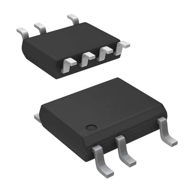
-
LNK304DN-TL Power Integrations
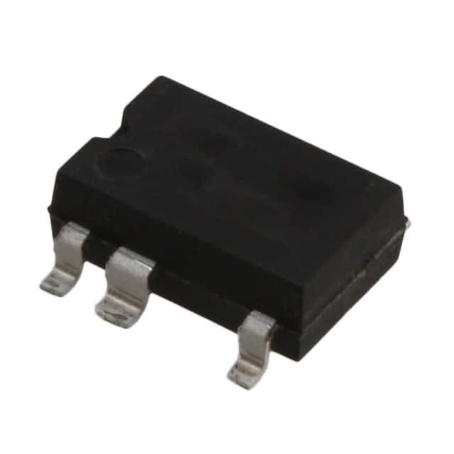
-
LNK304GN-TL Power Integrations
-
LNK304DG-TL Power Integrations
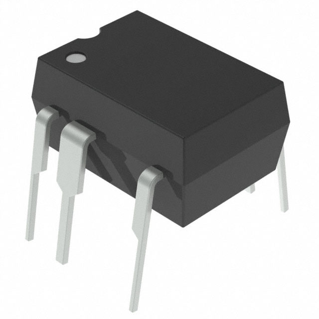
-
TNY277PN Power Integrations
-
TNY276PN Power Integrations
-
TNY278PN Power Integrations
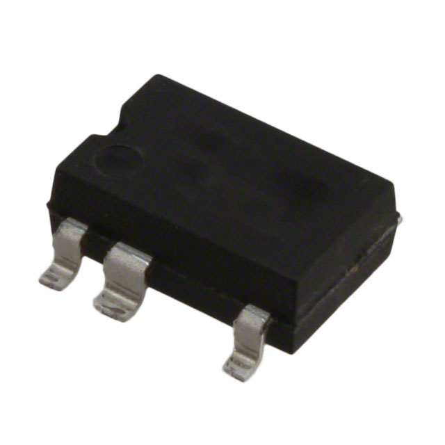
-
TNY278GN-TL Power Integrations
-
TNY280GN-TL Power Integrations
-
TOP266KG-TL Power Integrations
-
TOP258PN Power Integrations
-
TOP253PN Power Integrations
-
TOP253PNAU Power Integrations

- 1500+ Daily average RFQ Volume

- 20,000.000 Standard Product Unit

- 1800+ Worldwide Manufacturers

- 15,000+ In-stock Warehouse