N-Channel vs P-Channel MOSFETs: When to Use Which (And Why P-Ch Always Costs You RDS(on))
N-Channel vs P-Channel MOSFETs: When to Use Which (And Why P-Ch Always Costs You RDS(on))
The short answer: use N-channel for everything unless you're switching the high side. If you're switching the high side and your current is under 2A, use P-channel and accept the worse RDS(on) as the price of not needing a charge pump.
But the short answer hides a lot of "it depends." So let's go deeper — starting with the physics, because understanding why P-channel is worse tells you when it's still the right choice.
The Physics Tax: Why P-Channel RDS(on) Is Always 2–3× Higher
If you've ever browsed a MOSFET parametric table, you've noticed the pattern. For the same package and voltage rating, P-channel parts consistently have 2–3× higher RDS(on). A 30V N-channel in SOT-23 might do 24mΩ. The equivalent P-channel does 52mΩ. Same package, same manufacturer, same trench technology. Different physics.
The reason is carrier mobility. In silicon at room temperature:
- Electrons (N-channel carriers): μn ≈ 1,400 cm²/(V·s)
- Holes (P-channel carriers): μp ≈ 450 cm²/(V·s)
- Ratio: electrons move about 3.1× faster than holes
A "hole" isn't really a particle — it's the absence of an electron in the crystal lattice, and it "moves" by electrons hopping between adjacent atoms to fill it. This is inherently slower than an electron zipping through the conduction band. The on-resistance formula tells the story:
RDS(on) ∝ L / (W · μ · Cox · (VGS − Vth))
Lower mobility (μ) means higher RDS(on) per unit of die area. To match an N-channel MOSFET's on-resistance, a P-channel part needs roughly 3× the die area — which won't physically fit in the same package.
This isn't a design flaw. It's a material property of silicon. No manufacturer has "solved" it, because you can't change the carrier mobility of silicon without changing the semiconductor material entirely (SiC, GaN — different conversation, different price point).
The Gate Drive Problem: Why P-Channel Exists at All
So if P-channel is objectively worse on the spec sheet, why does anyone use it?
Because of the gate drive problem in high-side switching.
In a low-side switch, the MOSFET sits between the load and ground. The source is at 0V. To turn on an N-channel MOSFET, you drive the gate to 3.3V or 5V — VGS is positive, the FET turns on. Easy.
In a high-side switch, the MOSFET sits between the positive rail and the load. The source is at VIN (let's say 5V). To turn on an N-channel MOSFET, you need to drive the gate above VIN by at least VGS(th) — typically 3–5V above the rail. If VIN is 5V and VGS(th) is 1V, you need 6V+ at the gate. Your 3.3V MCU GPIO cannot generate 6V.
This is the single most common MOSFET mistake on electronics forums. The Arduino forums, EEVblog, and StackExchange are full of threads where someone used an N-channel MOSFET as a high-side switch driven directly from a 3.3V GPIO, and the MOSFET "doesn't work" or "gets hot." What's actually happening: the FET never fully turns on. It operates in the linear region. RDS(on) is orders of magnitude higher than the datasheet number. The designer blames the MOSFET. The MOSFET is fine. The topology is wrong.
And there's a second, sneakier failure: even when "off," the N-channel MOSFET's body diode is forward-biased from source to drain in the high-side position, keeping the load permanently powered. The FET literally cannot turn off the load, regardless of gate voltage. This catches beginners constantly because the body diode isn't shown on simplified MOSFET symbols.
Enter the P-channel MOSFET. Source at VIN (5V). Pull the gate to 0V, and VGS = -5V. The FET turns on — fully enhanced, low RDS(on). Your 3.3V MCU GPIO can do this directly: set the pin low. No charge pump. No bootstrap capacitor. No gate driver IC. Three components total: the MOSFET, a gate resistor, and a pull-up resistor to ensure the FET stays off during MCU reset.
Three Real MOSFETs, Three Real Jobs
Let's ground this in actual parts. Here's the NCE SOT-23 family — three MOSFETs, same package, same manufacturer, three completely different jobs:
| Parameter | NCE3400 | NCE2305 | NCE2302 |
|---|---|---|---|
| Channel | N-Channel | P-Channel | N-Channel |
| VDS | 30V | -20V | 20V |
| ID (continuous) | 5.8A | -4.1A | 2.9A |
| RDS(on) @ 4.5V | 24mΩ | 52mΩ | 33mΩ |
| Gate Charge (QG) | 10nC | 7.8nC | 4.0nC |
| Role | Workhorse | High-side specialist | Speed king |
NCE3400 (N-Ch, 30V/5.8A, 24mΩ): The workhorse. Best RDS(on) in the family, best current rating, best voltage rating. Use it for low-side switching, DC-DC converters, motor drivers, battery protection. If you don't know which one to use and you're switching the low side, start here.
NCE2305 (P-Ch, -20V/-4.1A, 52mΩ): The high-side specialist. Yes, the RDS(on) is more than double the NCE3400's. That's the physics tax — electrons are 3× faster than holes. At 2A, the NCE2305 drops 104mV in a high-side switch configuration vs 48mV for the NCE3400 on the low side. That 56mV difference is the price of eliminating a charge pump from your BOM. For loads under 2A, it's almost always the right trade.
NCE2302 (N-Ch, 20V/2.9A, 33mΩ, 4.0nC QG): The speed king. Less than half the gate charge of the NCE3400 means it switches more than twice as fast with the same gate drive current. At 500kHz PWM, the NCE3400's switching loss dominates and the part runs hot. The NCE2302, with 4.0nC QG, switches cleanly at 500kHz with a 10mA gate driver. The trade-off: lower voltage rating (20V) and lower current (2.9A).
The Decision Tree
Here's how to pick in 30 seconds:
- Are you switching the high side (positive rail)?
YES → P-channel (NCE2305). Don't fight the topology. A charge pump to drive a high-side N-channel costs more in BOM and PCB area than the P-channel's higher RDS(on) costs in efficiency, at currents below ~3A.
NO → continue to step 2. - Is your drain voltage above 20V, or load current above 3A?
YES → NCE3400. You need the voltage and current headroom.
NO → continue to step 3. - Are you switching above 200kHz?
YES → NCE2302. Gate charge matters more than RDS(on) at high frequency.
NO → Either NCE2302 or NCE3400. NCE2302 costs less. NCE3400 gives you more design margin.
When the "Always Use N-Channel" Advice Is Wrong
There's a common piece of advice among experienced power electronics engineers: "always use N-channel MOSFETs." For DC-DC converters, motor drives, and anything above 10A, this is absolutely correct. N-channel devices are fundamentally better — lower RDS(on), faster switching, lower cost per amp.
But this advice gets cargo-culted into low-current designs where it doesn't apply. A USB power switch delivering 5V at 500mA doesn't need a bootstrap circuit and a gate driver IC. A P-channel MOSFET with 52mΩ RDS(on) drops 26mV at 500mA. The N-channel alternative — with gate driver — costs more, takes more board space, and has more failure points, for a 26mV improvement that doesn't matter. The right tool for 10A is the wrong tool for 500mA.
Common Mistakes
Driving a P-channel gate directly from 12V. Most SOT-23 P-channel MOSFETs have ±12V VGS max (the NCE2305 included). With source at 12V, pulling the gate to 0V gives VGS = -12V — right at the absolute maximum with zero safety margin. Add a zener clamp from gate to source, use a gate voltage divider, or pick a part with ±20V VGS rating (like the AO3401A).
Forgetting the gate pull-up on P-channel. During MCU reset or power-up, GPIOs float. Without a 10kΩ–100kΩ pull-up resistor from gate to source, the gate can drift to an intermediate voltage, leaving the FET partially on. This is a one-cent component. Add it.
Using N-channel on the high side without checking if the body diode is blocking. In a high-side N-channel configuration, the body diode points from source (at the load side) to drain (at the supply side). It conducts whenever the source is more positive than the drain — which is exactly what happens when you try to turn it off. The load stays powered through the body diode regardless of gate voltage. If your N-channel high-side switch "won't turn off," this is why.
The Bottom Line
N-channel MOSFETs are fundamentally better devices — lower RDS(on), higher current density, lower cost per amp. Use them everywhere you can. But the world contains high-side switches, and high-side switches are simpler with P-channel MOSFETs. Don't cargo-cult the "always N-channel" advice into designs where a P-channel is the simpler, cheaper, more reliable solution.
All three NCE SOT-23 MOSFETs — plus AO3400A, AO3401A, and the full P-channel alternative lineup — are in stock at ICMASS. Contact us for current pricing on your quantity. Shenzhen stock, same-day dispatch before 15:00 CST.
Tags: MOSFET selection, N-channel vs P-channel, high-side switching, SOT-23 MOSFET, gate drive, NCE3400, NCE2305, NCE2302, carrier mobility
Related information




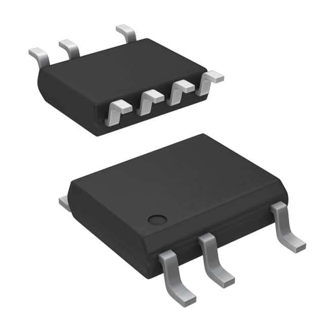
-
LNK304DN-TL Power Integrations
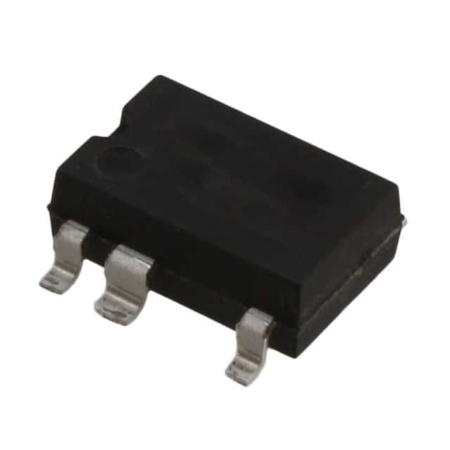
-
LNK304GN-TL Power Integrations
-
LNK304DG-TL Power Integrations
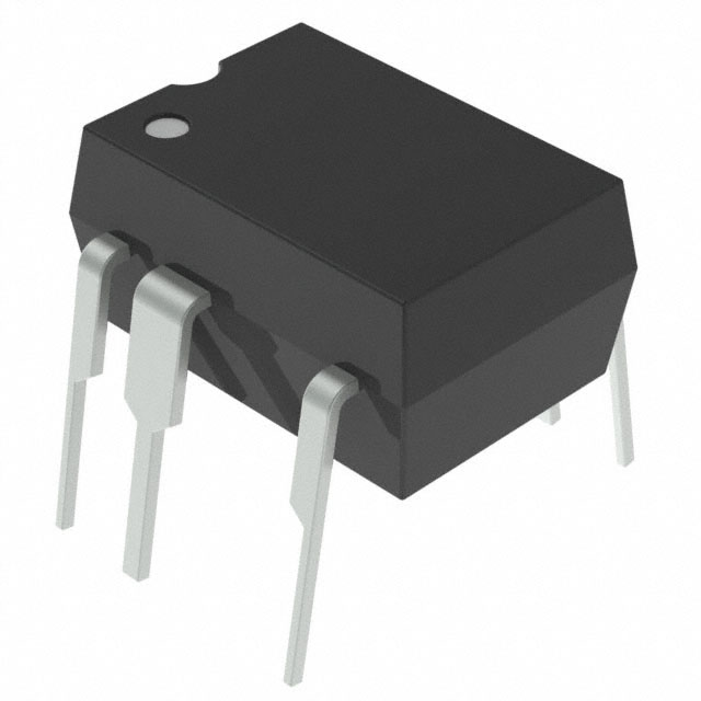
-
TNY277PN Power Integrations
-
TNY276PN Power Integrations
-
TNY278PN Power Integrations
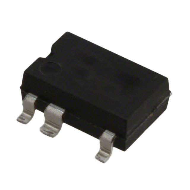
-
TNY278GN-TL Power Integrations
-
TNY280GN-TL Power Integrations
-
TOP266KG-TL Power Integrations
-
TOP258PN Power Integrations
-
TOP253PN Power Integrations
-
TOP253PNAU Power Integrations

- 1500+ Daily average RFQ Volume

- 20,000.000 Standard Product Unit

- 1800+ Worldwide Manufacturers

- 15,000+ In-stock Warehouse